Answer the question
In order to leave comments, you need to log in
How does the processor's clock signal generator work?
Tact
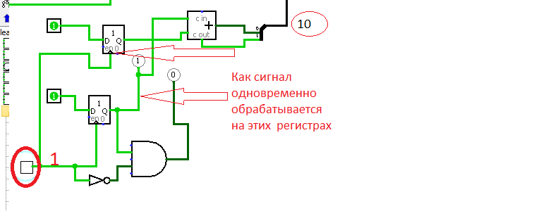
Here is a shorter example, I press the button, I give a signal, In the circuit, the signal passes to 2 registers and writes values \u200b\u200bto them, then sums them up.
The question is how they are simultaneously processed, THAT IS, here the signal arrived at 1 register, a value was written into it and transferred further to the adder. Then it should sum up, but (IN MY UNDERSTANDING) the 2nd register has not yet been processed, that is, at the time of processing 1 register, there is also 0. Then there should be 1 + 0 = 1, but the signal generator works differently (somehow at the same time), I did not find information on the issue, or missed something.
The task is to write a program to simulate the work of the Processor on Harvard Architecture.

And yet, do I understand correctly that the Control Bus is a wire in the circuits through which signals go from the clock generator to other sources?
And who else knows how the clock generator gives a signal, which I understood from a given time interval? But what happens if you send a signal faster than the previous signal had time to be processed? Or is Kalbek implemented there?
Answer the question
In order to leave comments, you need to log in
1. In your title - one question (about the clock generator), and in the text - a completely different one (about the operation of registers and the adder). In fact, you can answer both separately.
The clock generator is simply a source of periodic pulses of a standardized form, and it can be anything, as long as it gives what the rest of the processor requires. Sometimes additional requirements are imposed on it - say, a stable frequency, or two time-shifted series of pulses (two-phase).
The adder is a combinational logic that does not need clock pulses from any side. Operands were sent to the inputs, and after the delay time, the sum was received at the output. And the registers are not so, their state depends not only on the current signals, but also on what happened before (the so-called sequential logic). Moreover, often the triggers that make up the registers can be built in such a way as to use not only the fronts of the clock pulses, but also their recessions. In your case, it is enough to apply the initial operands to the D-inputs of the registers, and then simultaneously to both counting inputs - a clock pulse. After a delay, the sum is formed at the output of the adder. What difficulties scared you in this simple process, I do not understand.
2. The control bus contains not only a clock transmission line, but also other lines that transmit other signals - for example, write / read signals of I / O ports and memory, interrupt signals (there are several different types), processor service signals (say, transfer to step-by-step mode), well, etc.
But what happens if you send a signal faster than the previous signal had time to be processed?3. There will be a failure, because by supplying a clock pulse earlier than the state of the digital circuit has settled down from the previous pulse, i.e. by actually reducing the period of the clock sequence, you are trying to operate with who knows what. If the processor requires reliable operation without errors, then it is impossible to reduce the clock period (or, in other words, exceed the clock frequency relative to its nominal value).
Didn't find what you were looking for?
Ask your questionAsk a Question
731 491 924 answers to any question