Answer the question
In order to leave comments, you need to log in
How to apply a positive voltage to the transistor gate if there are many signal sources and they radically differ in signal?
Hello.
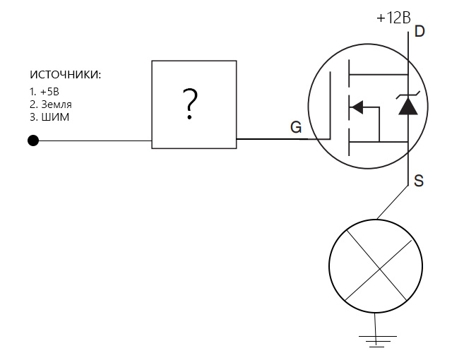
I ask you to suggest a radio element or radio elements to create a positive voltage on the gate of the N channel transistor. Better yet, show me the diagram.
Given.
• N channel Mosfet, for switching 10A
• One of the options for the signal source (for example, now the MK is working with PWM, after five minutes, the MK turned off and the signal became + 5V):
Answer the question
In order to leave comments, you need to log in
Now acceptable, except for a typo shorting Q1's base and emitter, and its incorrect conduction type - it should be NPN with the specified power polarity, but ... again, the devil is in the details.
1. Transistor Q1 is just a repeater here, i.e. the emitter/gate will have what is applied to the base, but 0.7 volts lower (this is the standard drop on a silicon PN junction). From this it is easy to deduce that Q1 can be dispensed with. It is needed only if a very sharp opening of Q2 is required, in tens of nanoseconds, and this is not always required. And from the source of the control signal, such a sharp drop is not easy to provide.
2. Again, it is not clear why you are listing your 3 points. +12 volts is the correct control signal, and if the gate voltage is raised gradually, then at the moment of transition through 3 ... 4 volts, the key will open quite sharply (this is the opening threshold - Upor). These 12 volts are more than this Upor, this is required to reduce the resistance of the public key channel, while transistor Q2 heats up less. But it should not be more than 15 ... 18 volts, otherwise there will be a breakdown of the gate per channel. Ground is not a control signal, but the base level from which the rest of the signals are measured - zero volts. When applying 0 volts to the shutter, the key is guaranteed to be closed. Well, PWM is just pulses that should open the key, and therefore, their amplitude should not be lower than Upor, but rather the same 12 volts. The pauses between them are still the same 0 volts, the key is closed in pauses. So there are no three directorates, but only one.

Either switch 0 loads with an n-channel one (left picture), or use a p-channel transistor (right picture).
match the ground at the sources and tie it to the potential at S of the MOSFET.
get a standard circuit with a common source.
if between G and S the voltage exceeds the maximum value from the datasheet to the MOS transistor, then plug a zener diode there, put a current-limiting resistor of 10-20 kΩ in series with it between the zener diode and signal sources.
I understand that you have S tied to the ground. With respect to it, you apply either +5 V or +12 V ??
Robyaty) It looks like I thought of it. It seems to be simple.
Please take a look, right?
Nothing puffs up?
Will the device consume something when the mosfet is closed?
Will the mosfet open from +5, +12? from the earth? from PWM?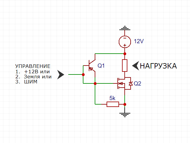
Didn't find what you were looking for?
Ask your questionAsk a Question
731 491 924 answers to any question