Answer the question
In order to leave comments, you need to log in
An error in the RAM 16x1 scheme in the book “Code. Secret language of informatics” or my inattention?
Good day. Help, please, deal with the problem. I was stumped while reading Code: The Secret Language of Computer Science by Charles Petzold. The problem is that I couldn't find the logic in some of the circuits that show memory logic. I have already checked the circuits several times and could not find the logic in some places, but at the same time I very much doubt that there can be such a mistake in such a high-quality, popular and old book.
I would like to briefly explain the situation, but it will not work. I'll start where this chapter begins. There is a latch that stores one bit of information, it looks like this:
This latch has 2 inputs DI(data input) and W(write) and one output DO(data output). A signal at input W means that the value of the signal at input DI must be written to output DO. If the signal on W is 1, on DI is 0, then the output DO will be “stored” 0. If the signal on W is 1, on DI is 1, then the output DO will be “stored” 1. If the signal on W is “0 ", then the last "written" value will be stored in DO, even if the DI signal changes. The latch logic table looks like this: 
Eight 1-bit latches can be assembled into an eight-bit one. To do this, you need to connect their Write(W) inputs: 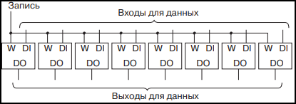
An eight-bit latch has 8 data inputs, 8 outputs, the only Write input, normally equal to 0. In order to store 8 bits of information, the Write input is fed 1, and then again 0 ,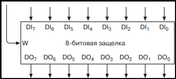
Or like this: 
With the help of such a latch, each bit cannot be recorded separately, only all together.
It is necessary to make it possible to write information to any selected latch of the eight available, separately from the other seven, at any time, without erasing information from others, and also to read separately. For this task, a 3 to 8 decoder and an 8 to 1 selector are used. The 3 to 8
decoder looks like this: 
By changing the address (switching switches), we can choose which of the 8 latches the information will be written to. The logic table for this decoder looks like this: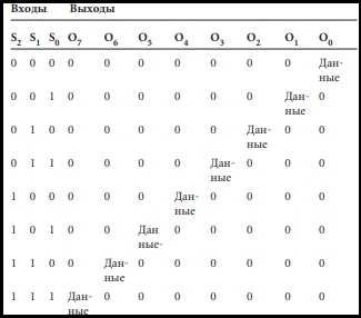
The Write signal must be fed to a 3 to 8 decoder, using the switches you can select one of the 8 latches to which the signal from the decoder will pass, and it is to this latch that the Write signal will pass.
The Data Input (DI) signal will be the same for all latches, because the Write signal will only go to one, so the rest will not be affected in any way.
At the end is an 8 by 1 selector: 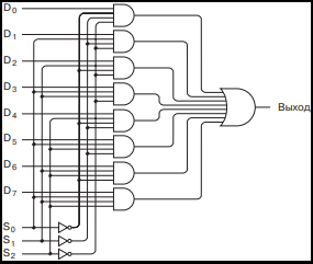
It works much like a decoder, selects the signal from one of the 8 latches, the signal from which will be fed to the output (“bulb”). The same 3 signals of the Address (switches) are fed to the selector as to the decoder, so if you select, for example, 6 latch using the address (switches), then 6 latch will be selected on both the decoder and the selector.
If you need to write information, then any latch is selected, a signal is applied to the Data Input (DI) - 0 or 1 and the Record button is pressed, the signal from the Data Input (DI) input is “written” to the selected latch. Or if you want to read the information, then any latch is selected, if the light is on, then 1 is written to this latch, if not, then 0.
Thus, we got an 8x1 RAM array that can store 8 different values. Here is the finished circuit: 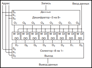
Then comes the circuit that made me mentally suffer: 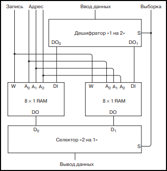
If you connect two eight-bit latches, you get 16x1 memory. There is a 1 to 2 decoder here that selects one of two 8x1 RAM arrays using the Select switch. The sample is the 4th switch (address).
Now pay attention to the fact that the Record signals and the switch signal (Address) go to both arrays. Imagine that using the Select switch, for example, the left array is selected, the latch in this array is selected using the address 6, signal 1 is applied to the Data Input and the record button is pressed. Recall that the Record and Address signals are also transmitted to the right array (at least it is shown in the diagram), but there is no Data Input signal, that is, 0, because the signal is sent only to the left array, it turns out that when the Record button is pressed, the signal will go to both arrays, 1 will be written to the 6th latch in the left array, and 0 to the left. It turns out that values are written to two arrays at once, because 1 could be written in the 6th latch of the right array, and it was erased by writing information to 6 -th latch of another array.
I have an assumption that the Sampling switch should choose not only where the signal goes from the Data input, but also from the Record input.
Maybe that's the way it should be, but that doesn't make it any easier for me. I'm probably just dumb. Or maybe there really is a mistake? This book is online, so you can read more.
Answer the question
In order to leave comments, you need to log in
Didn't find what you were looking for?
Ask your questionAsk a Question
731 491 924 answers to any question