Answer the question
In order to leave comments, you need to log in
How to properly connect ATiny13 for firmware?
Good day to you, brothers.
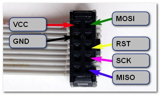
I want to program the MK, tell me, please, did I understand the meaning of the pins correctly and will it always be like this for all MKs (6 pins for programming)?
VCC - plus
GND - minus
RST - signaling the register to put the MK into write mode?
SCK - port responsible for the frequency (data recording speed in microns)?
MOSI - sending 1 bit per 1 cycle (hertz) from the programmer to the MK?
MISO - sending back from the MK to the programmer the same bit on the next cycle to check the correctness of the bit received before?
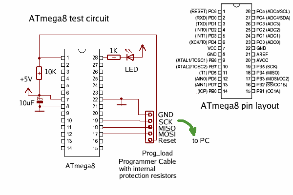
On the 2nd picture, resistors, a capacitor and an LED are added, is this mandatory or can I directly throw all 6 wires from the programmer to the MK (ATiny13)?
And what does the rest of the symbols in brackets mean?
For example (PCINT4/ADC2) and (MISO/AIN1/OC0B/INT0/PCINT1)?
There is a good book on the basics of programming MK (avr), otherwise there are articles either for advanced or unfinished ones.


Answer the question
In order to leave comments, you need to log in
The microcircuit has only 8 legs, so many are used for various purposes in different operating modes (multiplexing). What you are describing is the SPI protocol.
SCK - reference frequency for the SPI protocol. On this line, the programmer sends a periodic square-wave signal of a fixed frequency to synchronize the data transfer
MOSI (Master Output Slave Input) - a data transmission channel from the master device (programmer) to the slave (atmega)
MOSI - on the contrary
RST - a reset (reboot) signal. Can be used to transfer the chip to the desired state.
Everything else - you'll figure it out during development. As far as I know, INT * - interrupts (in order to respond to external events), ADC - digital-to-analog converter (measure voltage, all sorts of sensors)
Didn't find what you were looking for?
Ask your questionAsk a Question
731 491 924 answers to any question