Answer the question
In order to leave comments, you need to log in
Did I understand the timing diagram correctly?
Greetings!
There is a thermal head: 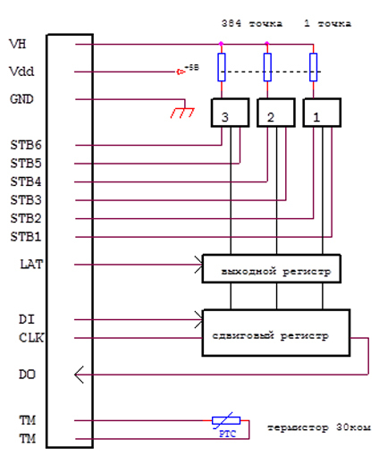
For control, there is such a timing diagram: 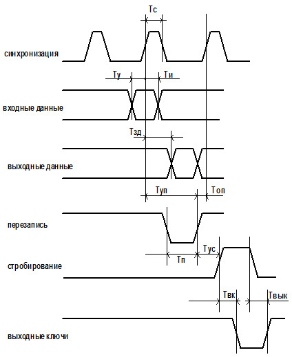
I connect to Arduino, I do this:
1. Set the level of the input data pin (0 or 1 as I need)
2. Wait 10 ms
3. Set the high level of the synchronization pin
4. wait 10ms
5 Set the sync pin low
6. loop 1-5 until all data has been sent
7. Set the overwrite pin low
8. wait 10ms
9. Set the overwrite pin high
10. wait 10ms
11. Set the gating pin high
12. wait 10 ms
13. Set the gating pin low
14. Loop 11-13 for strobe all 6 pins of strobes
Although in the end it works, it gives out garbage, according to which I cannot understand exactly where I made a mistake.
Answer the question
In order to leave comments, you need to log in
Not this way.
Data is loaded into the shift register block by block on the rising edge of the clock signal.
Roughly speaking, connect DI to MOSI (SPI), CLK to SCK (SPI), load some number of bytes (I would assume it will be either (384/3 = 128 bits) or (384 / 6 = 64 bits ). That is, 16 or 8 bytes. You can also load 16, the extra ones will be pushed out of the register. I advise you to load the value 0x55 - this way pixels will be visible through one.
Then set the LATCH strobe (pull it down) for an arbitrary time (it is enough to put the commands next to reset and set the pin.) Give the select command to the
corresponding keys - STB1~STB6 for
a
given
time .
Didn't find what you were looking for?
Ask your questionAsk a Question
731 491 924 answers to any question